

Class 12 Physics Notes: Band Theory & Semiconductors
Master Band Theory & Doping: High-Yield Notes for NEET & Board Exams

1. Introduction to Band Theory of Solids
Definition: Band theory explains the electrical behavior of solids based on the energy levels of electrons. It describes how isolated atomic energy levels transform when atoms are packed closely together to form a solid.
The Theory:
Isolated Atoms: In a single isolated atom, electrons occupy discrete (specific) energy levels.
Solid Formation: When atoms come together to form a solid, they interact. The outer electrons of neighboring atoms influence each other.
Energy Splitting: This interaction causes the single energy levels to split into millions of closely spaced energy levels.
Energy Bands: These closely spaced levels form continuous ranges called Energy Bands.
Key Concept: We no longer look at discrete lines for electron energy, but rather broad “bands” of allowed energy.
2. Classification of Energy Bands
There are two primary bands relevant to electrical conductivity:
A. Valence Band (VB)
This is the lower energy band.
It contains the valence electrons (outermost electrons).
These electrons are involved in chemical bonding and are generally bound to the nucleus.
State: Usually filled or partially filled with electrons.
B. Conduction Band (CB)
This is the higher energy band.
It contains electrons that have gained enough energy to break free from the atom.
These electrons are “free” and are responsible for electrical conduction.
State: Can be empty or partially filled.
C. Forbidden Energy Gap (Band Gap, Eg)
The energy difference between the top of the Valence Band and the bottom of the Conduction Band.
No electrons can exist in this gap.
Significance: An electron must gain energy equal to or greater than the Band Gap (Eg) to jump from the Valence Band to the Conduction Band.
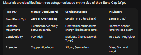
3. Classification of Materials Based on Band Theory
Materials are classified into three categories based on the size of their Band Gap
4. Charge Carriers in Semiconductors
Unlike metals, which only use electrons for conduction, semiconductors use two types of charge carriers.
1. Electrons (Negative Charge)
Located in the Conduction Band.
They move towards the positive terminal when an electric field is applied.
2. Holes (Positive Charge)
Definition: A “Hole” is simply the absence of an electron in the Valence Band.
Creation: When an electron jumps to the Conduction Band, it leaves a vacancy behind. This vacancy is the hole.
Movement: Holes behave like positively charged particles. When a neighboring electron moves to fill a hole, the hole effectively moves in the opposite direction.
Current: Holes move towards the negative terminal (in the direction of the Electric Field).
5. Types of Semiconductors
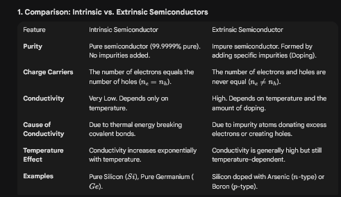
A. Intrinsic Semiconductors (Pure)
These are pure materials (e.g., pure Silicon or Germanium) without any impurities.
Charge Carriers: The number of electrons (n_e) is exactly equal to the number of holes (n_h).
n_e = n_h
Conductivity: Low at room temperature. Conductivity depends entirely on thermal excitation (heat) breaking bonds to create electron-hole pairs.
B. Extrinsic Semiconductors (Doped)
To improve conductivity, impurities are added to intrinsic semiconductors. This process is called Doping.
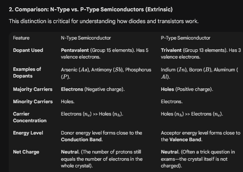
1. N-Type Semiconductor
Dopant: Pentavalent impurity (5 valence electrons) like Arsenic (As) or Antimony (Sb).
Mechanism: 4 electrons form bonds with Silicon; the 5th electron is loosely bound and easily enters the conduction band.
Majority Carrier: Electrons.
Minority Carrier: Holes.
Energy Level: Donor energy levels appear just below the Conduction Band.
2. P-Type Semiconductor
Dopant: Trivalent impurity (3 valence electrons) like Boron (B) or Aluminum (Al).
Mechanism: 3 electrons form bonds; the “missing” 4th bond creates a vacancy (Hole).
Majority Carrier: Holes.
Minority Carrier: Electrons.
Energy Level: Acceptor energy levels appear just above the Valence Band.
6. Factors Affecting Conductivity
A. Effect of Temperature
Semiconductors: As temperature increases, more covalent bonds break, and more electrons jump to the conduction band.
Result: Conductivity increases (Resistivity decreases).
Note: The Band Gap slightly decreases as temperature rises.
Metals: As temperature increases, atoms vibrate more, obstructing electron flow.
Result: Conductivity decreases.
B. Effect of Doping
Doping introduces new energy levels within the band gap.
N-type: Donor levels help electrons jump to the conduction band easily.
P-type: Acceptor levels help electrons leave the valence band easily (creating holes).
Even a tiny amount of doping significantly reduces the effective energy required for conduction, massively increasing conductivity.
📝 Summary for Exams
Band Theory: Interaction of atoms creates Valence (bound) and Conduction (free) bands.
Band Gap (Eg): The energy hurdle electrons must jump.
Metals: No gap.
Semiconductors: Small gap.
Insulators: Huge gap.
Holes: Vacancies in the valence band that act as positive charge carriers.
Doping: Adding impurities to control conductivity.
Pentavalent → N-Type (More electrons).
Trivalent → P-Type (More holes).
Why is an N-type semiconductor neutral if it has “extra” electrons? This is a common conceptual question.
Answer: Although we add an impurity that provides an extra free electron for conduction, that impurity atom also has an extra proton in its nucleus compared to the silicon atom it replaced. Therefore, the total number of negative charges (electrons) still equals the total number of positive charges (protons) in the solid. The material remains electrically neutral.
15 Multiple Choice Questions (MCQs) based on the Physics notes above for your NEET/CBSE revision.
Q1. According to Band Theory, what is the primary reason for the formation of energy bands in solids? A) The high density of the material B) The interaction between outer electrons of neighboring atoms C) The absorption of thermal energy D) The presence of impurities in the crystal Answer: B) When atoms come close together, the interaction between their outer (valence) electrons causes discrete energy levels to split into continuous bands.
Q2. The energy gap between the Valence Band and the Conduction Band where no electrons can exist is called: A) Fermi Level B) Forbidden Energy Gap (Band Gap) C) Potential Barrier D) Depletion Region Answer: B) It is called the Forbidden Energy Gap or Band Gap (Eg).
Q3. Which of the following values represents the approximate Band Gap (Eg) for Silicon at room temperature? A) 0.7 eV B) 1.1 eV C) 5.4 eV D) 0 eV Answer: B) Silicon has a band gap of approximately 1.1 eV. (Germanium is ~0.7 eV).
Q4. How do metals differ from semiconductors regarding their energy bands? A) Metals have a large band gap (> 3 eV). B) Metals have a completely empty valence band. C) Metals have overlapping Valence and Conduction bands. D) Metals have a small band gap (~1 eV). Answer: C) In metals, the valence and conduction bands overlap, allowing free movement of electrons.
Q5. What happens to the conductivity of a semiconductor as temperature increases? A) It decreases. B) It remains constant. C) It increases. D) It first increases then decreases. Answer: C) Conductivity increases because heat energy breaks more covalent bonds, generating more charge carriers (electrons and holes).
Q6. A “Hole” in a semiconductor is best defined as: A) A positive proton moving in the nucleus. B) A vacant electron state in the Valence Band. C) An excess electron in the Conduction Band. D) A neutral particle. Answer: B) A hole is the vacancy left behind in the valence band when an electron jumps to the conduction band.
Q7. To obtain an N-Type semiconductor, which type of impurity must be added to pure Silicon? A) Trivalent (Group 13) B) Tetravalent (Group 14) C) Pentavalent (Group 15) D) Monovalent (Group 1) Answer: C) Pentavalent elements (like Arsenic or Phosphorus) are used to provide extra electrons.
Q8. Which of the following is a Trivalent dopant used to create P-Type semiconductors? A) Phosphorus (P) B) Arsenic (As) C) Antimony (Sb) D) Boron (B) Answer: D) Boron is a Group 13 element with 3 valence electrons (Trivalent).
Q9. In an N-Type semiconductor, the majority charge carriers are: A) Holes B) Electrons C) Positive Ions D) Neutrons Answer: B) “N” stands for Negative; electrons are the majority carriers.
Q10. Where is the “Donor Energy Level” located in the energy band diagram of an N-Type semiconductor? A) Just above the Valence Band B) In the middle of the Band Gap C) Just below the Conduction Band D) Inside the Valence Band Answer: C) Donor levels are just below the Conduction Band so electrons can easily jump up.
Q11. What is the net electrical charge of a P-Type semiconductor crystal? A) Positive B) Negative C) Neutral D) Depends on the doping level Answer: C) Neutral. Even though it has more holes, the total number of protons equals the total number of electrons in the material.
Q12. In an Intrinsic (Pure) Semiconductor, which relationship is true regarding charge carrier concentration? A) n_e > n_h B) n_h > n_e C) n_e = n_h D) n_e = 0 Answer: C) In pure semiconductors, every electron that jumps creates exactly one hole, so their numbers are equal.
Q13. At Absolute Zero temperature (0 Kelvin), a pure semiconductor behaves as: A) A Superconductor B) A Perfect Conductor C) A Perfect Insulator D) A P-N Junction Answer: C) At 0 K, there is no thermal energy to lift electrons to the conduction band, so the conduction band is empty.
Q14. When an electric field is applied to a semiconductor, how do holes move? A) Towards the positive terminal B) Towards the negative terminal C) Randomly in all directions D) They do not move Answer: B) Holes act as positive charges, so they move towards the negative terminal (in the direction of the Electric Field).
Q15. Why does the resistance of a metal increase with temperature, unlike a semiconductor? A) The number of electrons decreases. B) The band gap increases. C) The vibration of atoms increases, causing more collisions. D) The electrons become heavier. Answer: C) In metals, increased thermal vibration of atoms obstructs the flow of free electrons, increasing resistance.
Here are 25 Fill-in-the-Blank questions derived from the notes above, designed for your practice.
Fill in the Blank Questions
According to Band Theory, the interaction of atoms in a solid causes discrete energy levels to split into continuous ranges called ______.
The energy band that contains the outermost electrons involved in bonding is called the ______ Band.
The energy band containing free electrons responsible for electrical conduction is known as the ______ Band.
The energy interval between the Valence Band and the Conduction Band where no electrons can exist is called the ______ Energy Gap.
In ______, the Valence Band and Conduction Band overlap, resulting in very high conductivity.
The approximate Band Gap (Eg) for Silicon at room temperature is ______ eV.
Insulators are characterized by a very ______ Band Gap, typically greater than 3 eV.
As the temperature of a semiconductor increases, its conductivity ______.
In contrast to semiconductors, the conductivity of a ______ decreases as temperature increases.
A vacancy created in the Valence Band when an electron jumps to the Conduction Band is called a ______.
Holes behave like ______ charged particles and move in the direction of the electric field.
A pure semiconductor free from any impurities is called an ______ semiconductor.
In an intrinsic semiconductor, the number of free electrons (ne) is always ______ to the number of holes (nh).
The process of adding specific impurities to a pure semiconductor to increase its conductivity is called ______.
______ semiconductors are formed by adding impurities to pure semiconductors.
To create an N-Type semiconductor, a ______ impurity (with 5 valence electrons) is added.
Common examples of pentavalent dopants include Arsenic and ______.
In an N-Type semiconductor, the majority charge carriers are ______.
To create a P-Type semiconductor, a ______ impurity (with 3 valence electrons) is added.
Boron and Aluminum are examples of ______ impurities used for P-type doping.
In a P-Type semiconductor, the majority charge carriers are ______.
In an N-Type semiconductor, the ______ energy level is located just below the Conduction Band.
In a P-Type semiconductor, the ______ energy level is located just above the Valence Band.
Despite having majority and minority carriers, a doped semiconductor crystal remains electrically ______.
At absolute zero temperature (0 Kelvin), a pure semiconductor behaves like a perfect ______.
Answer Key
Energy Bands
Valence
Conduction
Forbidden (or Band Gap)
Metals
1.1
Large
Increases
Metal
Hole
Positively
Intrinsic
Equal
Doping
Extrinsic
Pentavalent
Antimony (or Phosphorus)
Electrons
Trivalent
Trivalent (or Acceptor)
Holes
Donor
Acceptor
Neutral
Insulator
Here are 32 Assertion and Reasoning questions based on the notes.
Directions for all questions:
(A) Both Assertion and Reason are true and Reason is the correct explanation of Assertion.
(B) Both Assertion and Reason are true but Reason is NOT the correct explanation of Assertion.
(C) Assertion is true but Reason is false.
(D) Assertion is false but Reason is true.
Q1. Assertion (A): The electrical conductivity of a semiconductor increases with a rise in temperature.
Reason (R): Higher temperatures provide more thermal energy, breaking more covalent bonds and generating a larger number of electron-hole pairs.
Answer: (A)
Explanation: Heat energy excites electrons from the valence band to the conduction band. This creation of charge carriers increases conductivity.
Q2. Assertion (A): An N-type semiconductor is electrically neutral.
Reason (R): In N-type semiconductors, the number of free electrons (nₑ) is equal to the number of holes (nₕ).
Answer: (C)
Explanation: The Assertion is true (the material is neutral), but the Reason is false. In N-type, electrons are majority carriers, so nₑ >> nₕ.
Q3. Assertion (A): Metals have very high electrical conductivity.
Reason (R): In metals, the Valence Band and Conduction Band overlap, allowing electrons to move freely without needing to cross an energy gap.
Answer: (A)
Explanation: The lack of a band gap means electrons are always available for conduction.
Q4. Assertion (A): Pure Silicon is an insulator at Absolute Zero (0 Kelvin).
Reason (R): At 0 K, there is no thermal energy available to excite electrons across the band gap from the valence band to the conduction band.
Answer: (A)
Explanation: Without thermal energy, the conduction band remains empty, and no current can flow.
Q5. Assertion (A): Holes are considered positive charge carriers in semiconductors.
Reason (R): A hole acts as a positive charge because it represents the vacancy left by an electron in the valence band.
Answer: (A)
Explanation: The absence of a negative electron in a neutral lattice behaves effectively as a positive charge.
Q6. Assertion (A): Pentavalent impurities are used to create P-type semiconductors.
Reason (R): Pentavalent elements have 5 valence electrons.
Answer: (D)
Explanation: Assertion is false; Pentavalent impurities create N-type (Negative) semiconductors. The Reason is factually true (Group 15 elements have 5 valence electrons).
Q7. Assertion (A): Resistivity of metals increases with temperature.
Reason (R): With the increase in temperature, the collision frequency of electrons with the vibrating lattice ions increases.
Answer: (A)
Explanation: In metals, thermal vibrations obstruct the flow of free electrons, increasing resistance.
Q8. Assertion (A): In N-type semiconductors, the majority charge carriers are electrons.
Reason (R): Pentavalent dopants donate an extra electron to the conduction band.
Answer: (A)
Explanation: The extra electrons provided by the donor atoms become the majority carriers.
Q9. Assertion (A): Diamond is classified as an insulator.
Reason (R): Diamond has a very large Band Gap (Eg > 3 eV).
Answer: (A)
Explanation: A large band gap prevents electrons from jumping to the conduction band, making the material an insulator.
Q10. Assertion (A): Pure Silicon is an intrinsic semiconductor.
Reason (R): In pure Silicon, the number of electrons equals the number of holes (nₑ = nₕ).
Answer: (B)
Explanation: Both statements are true. Silicon is intrinsic because it is pure. The fact that nₑ = nₕ is a characteristic of intrinsic semiconductors, not the reason why Silicon is called intrinsic (it is called intrinsic because it is chemically pure).
Q11. Assertion (A): The donor energy level in an N-type semiconductor is located just below the Conduction Band.
Reason (R): The energy required to move the loosely bound fifth electron into the conduction band is very small.
Answer: (A)
Explanation: Because the fifth electron is loosely bound, its energy state is very close to the conduction band (approx 0.01 to 0.05 eV).
Q12. Assertion (A): Carbon (Diamond) and Silicon both have 4 valence electrons, but Carbon is an insulator while Silicon is a semiconductor.
Reason (R): The Band Gap of Carbon is much larger than that of Silicon.
Answer: (A)
Explanation: Despite similar valence structures, the tighter binding in Carbon creates a massive energy gap (~5.4 eV) compared to Silicon (~1.1 eV).
Q13. Assertion (A): Doping significantly increases the conductivity of a semiconductor.
Reason (R): Doping increases the number of charge carriers (either electrons or holes) without requiring high temperatures.
Answer: (A)
Explanation: Doping introduces available carriers at room temperature, drastically lowering resistivity.
Q14. Assertion (A): In a P-type semiconductor, the acceptor energy level is situated just above the Valence Band.
Reason (R): Electrons from the Valence Band can easily jump to the acceptor level, creating holes in the Valence Band.
Answer: (A)
Explanation: The acceptor level captures electrons easily because it is energetically very close to the valence band.
Q15. Assertion (A): The forbidden energy gap in Ge (Germanium) is smaller than in Si (Silicon).
Reason (R): Germanium has a higher atomic number and larger size, making the valence electrons less tightly bound to the nucleus.
Answer: (A)
Explanation: Ge (Gap ~0.7 eV) holds electrons less tightly than Si (Gap ~1.1 eV).
Q16. Assertion (A): An electric field applied to a semiconductor causes holes to move towards the positive terminal.
Reason (R): Holes act as positive charge carriers.
Answer: (D)
Explanation: Assertion is false. Since holes act as positive charges (Reason is true), they are repelled by the positive terminal and move towards the negative terminal.
Q17. Assertion (A): Energy bands in solids are formed due to the Pauli Exclusion Principle.
Reason (R): When atoms are close, electrons cannot occupy the same quantum states, so energy levels split.
Answer: (A)
Explanation: This is the fundamental quantum mechanical reason for band formation.
Q18. Assertion (A): Trivalent impurities like Indium are called “Acceptor” impurities.
Reason (R): They accept an electron from the host crystal’s valence band to complete their bonding, creating a hole.
Answer: (A)
Explanation: By accepting an electron, they create a vacancy (hole) in the lattice.
Q19. Assertion (A): The number of holes in a P-type semiconductor is always greater than the number of electrons.
Reason (R): In P-type semiconductors, holes are generated by doping, while electrons are only generated by thermal generation.
Answer: (A)
Explanation: Doping provides a massive surplus of holes (majority), while the few electrons (minority) only come from thermal bond breaking.
Q20. Assertion (A): Gallium Arsenide (GaAs) is a compound semiconductor.
Reason (R): It is formed by combining elements from Group 13 (Ga) and Group 15 (As).
Answer: (A)
Explanation: Unlike elemental semiconductors (Si, Ge), GaAs is a compound material widely used in electronics.
Directions for all questions:
(A) Both Assertion and Reason are true and Reason is the correct explanation of Assertion.
(B) Both Assertion and Reason are true but Reason is NOT the correct explanation of Assertion.
(C) Assertion is true but Reason is false.
(D) Assertion is false but Reason is true.
(E) Both Assertion and Reason are false.
Q1. Assertion (A): An N-type semiconductor is electrically neutral as a whole.
Reason (R): In N-type semiconductors, the number of electrons is exactly equal to the number of holes (ne=nh).
Answer: (C) Explanation: The assertion is true; the crystal is neutral because the total number of protons equals the total number of electrons. However, the reason is False because in N-type material, electrons are the majority (ne≫nh), so they are not equal.
Q2. Assertion (A): At absolute zero temperature (0 K), a pure semiconductor behaves like a perfect insulator.
Reason (R): At 0 K, the Conduction Band is completely filled with electrons. Answer: (C)
Explanation: The assertion is true. However, the reason is False. At 0 K, the Conduction Band is completely empty, not filled. The Valence Band is filled.
Q3. Assertion (A): When Indium is added to Silicon, the resulting semiconductor is P-Type.
Reason (R): Indium acts as a Donor impurity and provides free electrons.
Answer: (C) Explanation: Indium is a Trivalent (Group 13) element, so it creates P-Type silicon (Assertion is True). However, Trivalent atoms are Acceptors, not Donors, and they create holes, not free electrons (Reason is False).
Q4. Assertion (A): The conductivity of a semiconductor increases significantly with temperature.
Reason (R): Increasing temperature increases the Band Gap (Eg) of the material.
Answer: (C) Explanation: Conductivity does increase with temperature (Assertion True). However, the band gap actually decreases slightly with temperature (Reason False). The main reason for increased conductivity is the breaking of covalent bonds, not the change in gap size.
Q5. Assertion (A): In a semiconductor, electric current is carried solely by electrons.
Reason (R): Holes in the valence band behave as positive charge carriers and contribute to current flow.
Answer: (D) Explanation: The assertion is False because current in semiconductors is carried by both electrons and holes. The reason is True: holes do contribute to current.
Q6. Assertion (A): The Band Gap of Diamond is smaller than that of Silicon.
Reason (R): Diamond is an insulator, whereas Silicon is a semiconductor.
Answer: (D) Explanation: The assertion is False; Diamond has a much larger band gap (~5.4 eV) than Silicon (~1.1 eV). The reason is True: Diamond is indeed an insulator and Silicon is a semiconductor.
Q7. Assertion (A): When an electric field is applied across a semiconductor, holes move towards the positive terminal.
Reason (R): Holes are considered to have a positive charge.
Answer: (D) Explanation: The assertion is False. Since holes act as positive charges (Reason is True), they are repelled by the positive terminal and move towards the negative terminal.
Q8. Assertion (A): Pure Silicon conducts electricity better than Copper at room temperature. Reason (R): Copper has overlapping Valence and Conduction bands.
Answer: (D) Explanation: The assertion is False; Copper (a metal) conducts much better than Silicon. The reason is True: metals like copper have overlapping bands, which is why they are such good conductors.
Q9. Assertion (A): Doping pure Silicon with Arsenic results in a P-Type semiconductor.
Reason (R): Arsenic is a Trivalent impurity with 3 valence electrons. Answer: (E)
Explanation: Both are False. Arsenic is a Pentavalent impurity (5 valence electrons), and doping with it creates an N-Type semiconductor.
Q10. Assertion (A): The Forbidden Energy Gap for metals is very large (approx 3 eV). Reason (R): Electrons in metals are tightly bound to the nucleus and cannot move freely.
Answer: (E) Explanation: Both are False. Metals have zero energy gap (overlapping bands), and their valence electrons are very loosely bound and move freely.
Q11. Assertion (A): In an Intrinsic semiconductor, doping is required to maintain the balance between electrons and holes.
Reason (R): Intrinsic semiconductors have high conductivity at 0 Kelvin.
Answer: (E) Explanation: Both are False. Intrinsic means “pure,” so no doping is involved (and n_e automatically equals n_h). At 0 Kelvin, intrinsic semiconductors have zero conductivity.
Q12. Assertion (A): A “Hole” is a physical particle located in the nucleus of the atom. Reason (R): Holes are protons that have been released from the nucleus during doping.
Answer: (E) Explanation: Both are False. A hole is not a nuclear particle; it is a “vacancy” in the electron structure of the Valence Band. Protons never leave the nucleus in semiconductor physics.
3-Marker Theory Questions for Class 12 Physics based on Band Theory and Semiconductors, along with their model answers.
Q1. Distinguish between Conductors (Metals), Semiconductors, and Insulators on the basis of Energy Band Theory.
Answer:
Based on the Band Theory of solids, materials are classified by the energy gap (Eg) between their Valence Band (VB) and Conduction Band (CB).
Metals (Conductors):
Band Structure: The Valence Band and Conduction Band overlap with each other. There is no forbidden energy gap (Eg ≈ 0).
Conductivity: Because the bands overlap, electrons from the valence band can easily move into the conduction band and are available for electrical conduction. Hence, they have very high conductivity.
Example: Copper, Aluminum.
Semiconductors:
Band Structure: There is a small forbidden energy gap between the valence and conduction bands (Eg < 3 eV). For Silicon, Eg is roughly 1.1 eV.
Conductivity: At 0 K, electrons cannot jump this gap, so they act as insulators. At room temperature, some electrons gain thermal energy to jump to the conduction band, allowing moderate conductivity.
Example: Silicon (Si), Germanium (Ge).
Insulators:
Band Structure: There is a very large forbidden energy gap (Eg > 3 eV).
Conductivity: The gap is so wide that even at high temperatures, electrons cannot acquire enough energy to jump from the valence to the conduction band. Thus, the conduction band remains empty, resulting in negligible conductivity.
Example: Diamond, Wood, Glass.
Q2. What is an Extrinsic Semiconductor? Explain the formation of an N-Type semiconductor with the help of an energy band diagram.
Answer:
Extrinsic Semiconductor:
A semiconductor whose conductivity is increased by adding a small amount of suitable impurity (dopant) is called an extrinsic semiconductor. This process is called doping.
Formation of N-Type Semiconductor:
Doping: When a pure semiconductor (like Silicon, Group 14) is doped with a Pentavalent impurity (Group 15 elements like Arsenic or Phosphorus).
Mechanism: The pentavalent atom has 5 valence electrons. 4 of these form covalent bonds with the neighboring 4 Silicon atoms. The 5th electron remains loosely bound to the nucleus and does not participate in bonding.
Conductivity: A very small amount of energy is required to detach this 5th electron. It easily jumps into the conduction band and becomes a free electron.
Majority Carriers: Since the impurity contributes extra electrons, electrons become the majority charge carriers, and holes are the minority carriers.
Energy Band Diagram: The pentavalent impurity introduces a new energy level called the Donor Level. This level is located just below the Conduction Band. Electrons from this donor level can easily move into the conduction band.
Q3. Explain the term ‘Hole’ in semiconductor physics. Why does a pure semiconductor behave as an insulator at Absolute Zero (0 K)?
Answer:
Concept of Hole:
A Hole is defined as a vacant energy state in the Valence Band of a semiconductor.
When an electron in the valence band gains sufficient energy (thermal or external) to jump into the conduction band, it leaves behind a vacancy. This vacancy is called a hole.
It behaves effectively as a positive charge carrier. Under the influence of an electric field, while electrons move towards the positive terminal, holes appear to move towards the negative terminal.
Behavior at Absolute Zero (0 K):
At Absolute Zero temperature (0 K), there is no thermal energy available to the electrons.
Without thermal energy, no covalent bonds are broken, and no electrons can jump from the Valence Band to the Conduction Band across the forbidden energy gap.
Consequently, the Conduction Band remains completely empty, and the Valence Band remains completely filled.
Since there are no free charge carriers available for conduction, a pure semiconductor behaves like a perfect insulator at 0 K.